Extreme Ultraviolet Mirror (EUV mirror)
Extreme Ultraviolet Mirror (EUV mirror) Series
FAQs
EUV stands for Extreme Ultraviolet, referring to electromagnetic waves with wavelengths from 10 nm to 124 nm. In semiconductor lithography, it specifically means 13.5 nm light, which is currently the only EUV source usable for mass‐production of chips.
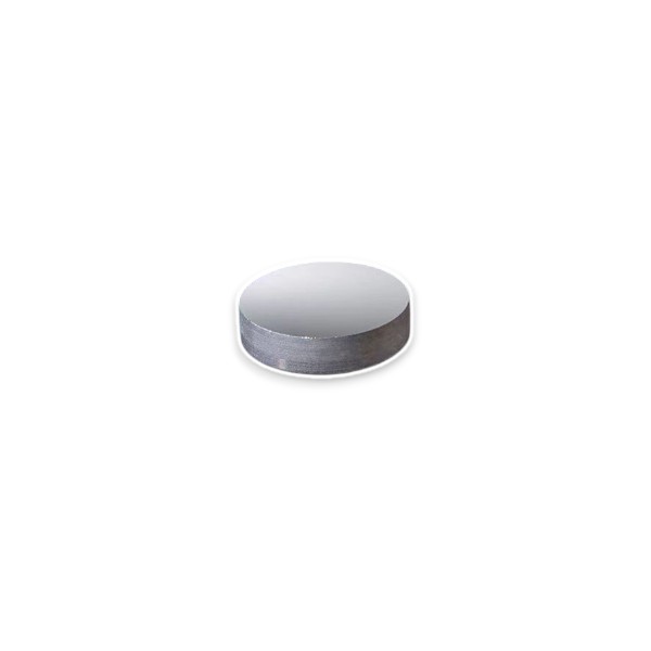
An EUV multilayer mirror is an optical element made by alternately stacking nanoscale thin films of two materials (such as silicon and molybdenum) to efficiently reflect extreme ultraviolet light. Its operation relies on constructive interference: by pairing materials with contrasting refractive indices and precisely controlling the thickness and number of layers, the mirror achieves high reflectivity at 13.5 nm.
EUV mirrors are the core components of an EUV lithography machine; without them, the optical path cannot transmit EUV light. An EUV lithography system uses about 10–12 such mirrors to repeatedly reflect and focus the EUV light from the source, ultimately projecting the mask pattern onto the silicon wafer. Because EUV is absorbed by conventional lens materials, mirrors are the only feasible optical solution.
EUV mirrors are primarily made by alternately stacking silicon (Si) and molybdenum (Mo) to form a multilayer film structure. Silicon and molybdenum are chosen because, at 13.5 nm wavelength, they have complementary optical properties that maximize the interference effect. Additionally, both Si and Mo have low thermal expansion coefficients and can withstand the thermal load of high‐power EUV sources (e.g., a 250 W laser plasma).
EUV mirrors are mainly used in semiconductor manufacturing (chip processing), scientific research (EUV microscopy and space exploration), and the EUV lithography machine industry.